Scanning Electron Microscopy & SEM-EDX | SEM-EDX Analysis
-
22 October 2023
-
Matt Calveley
Senior Materials Engineer at EA Technology, Matt Calveley, explores the use of Scanning Electron Microscopy and SEM-EDX as a tool for failure analysis and inspection.
For centuries, microscopes have provided us with the ability to explore the micro world. Whether that was the hidden aspects of the natural world, identifying harmful germs or as a tool to help us better understand the building blocks of the materials around us.
Up until the early 20th century, the ability to view this micro world was limited to the physical laws of light. However, in 1935 the first scanning microscope, using electrons as a source, was made possible by German scientist Max Knoll. This enabled a step forward in materials research and provided a new set of tools for failure investigation. In this article, we explore some of the uses for Scanning Electron Microscopy and, in particular, applications using SEM-EDX.
The Limits of Optical Microscopy
Although optical microscopy is one of the oldest tools in modern science (and is still incredibly useful today), it is limited in its ability to resolve distinct features when reaching higher magnification. The reason for this is to do with the principles of diffraction and the limitations of the natural wavelength of light. The 3D sense of objects (depth of field) is also limited in optical microscopy. This is particularly a problem at high magnifications, where the field of focus is very thin. The 3D sense of depth is greatly improved in real-time using Scanning Electron Microscopy. In addition, optical aberrations such as glare, caused by the interaction of light on shiny samples, are eliminated.
What is Scanning Electron Microscopy (SEM)?
In Scanning Electron Microscopy (SEM), samples are housed in a vacuum chamber which allows it to interact with a highly focused beam of electrons, continuously scanning over the sample. At the point where the beam hits the sample, the beam penetrates some depth into the surface of a sample and interacts with its atoms. The extent (depth) of interaction depends on many variables, but essentially the signal of the incident beams helps generate different information from the sample including topographical features and characteristic X-rays (elemental information).
What is SEM-EDX?
SEM-EDX analysis is short for Scanning Electron Microscopy Energy Dispersive X-ray analysis. It is sometimes called EDS or Energy Dispersive Spectroscopy. SEM-EDX is a process used by many electron microscopes where characteristic elemental X-rays are captured at a detector and analysed using software to create a spectrum. The X-rays contain specific energies that can be mapped to electrons within specific shells (energy levels) within different elements. The count number of the X-rays generated provides an indication of the proportion of different elements in a sample and this information can be used for identification of different materials and trace elemental features.
SEM-EDX for Failure Analysis
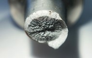
Scanning Electron Microscopy is a great tool for failure analysis. It can be used to examine broken parts and to identify different mechanisms of failure (distinguishing the difference between a slow progressive fracture and rapid, instantaneous failure for example). SEM-EDX can be used to help identify crack-causing features such as segregation and non-metallic inclusions within metals too.
SEM-EDX for Corrosion Analysis
Corrosion is a function of material and environment. SEM-EDX can be used to help identify the grade of materials in a given environment, assessing their suitability for different applications and it can also be used to identify contaminants that have caused corrosion to occur. Cross sections of corrosion scales can be prepared to identify the distribution of elements and to locate aggressive elements at the metal/scale interface.
SEM-EDX for Condition Assessment and Debris Analysis
During processes such as normal wear, or as a result of catastrophic failure, small fragments of metal may be generated. Under conditions where small amounts of material (particularly mixed material) exist, it may be impossible to analyse using bulk methods. In this situation, the pinpoint accuracy of an electron beam in combination with SEM-EDX may be the best method. Depending on the amount of material present, it may be possible to match fragments to components.
SEM-EDX for Coating Analysis
SEM-EDX can be used for analysis of paint flakes and coating. This might include assessing different layers within the paint for the presence and distribution of elements such as copper (used in bio-fouling resistant coatings) or lead.
SEM-EDX for Reverse Engineering
SEM-EDX can be used to help identify the grade of metal from small turnings of material. This is useful in the reverse engineering of large components or in the research and investigation of fine art artefacts.
SEM-EDX for contamination Analysis
SEM-EDX can be used for the identification and quantification of particles that may be part of contamination. This has applications in engineering and fuel analysis but has also been used for the identification of microplastics.
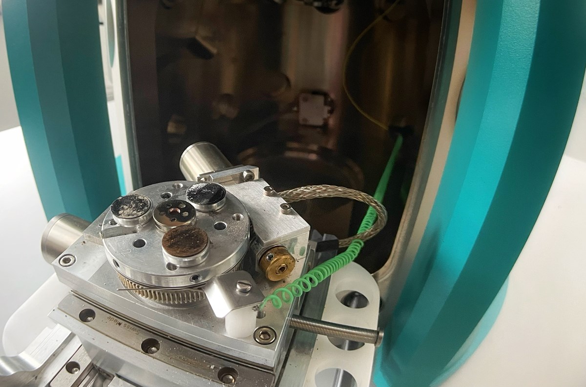
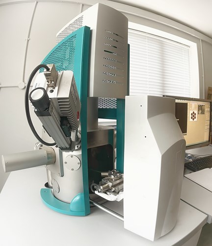
EA Technology has a dedicated Scanning Electron Microscopy suite with SEM-EDX capabilities which are available for independent analysis of samples. If you would like to learn more about our SEM-EDX capabilities, please contact our Forensics team here.
You can read Matt’s previous blog on Material Testing for Quality Assurance, Failure Investigation, and Condition Assessment here.